

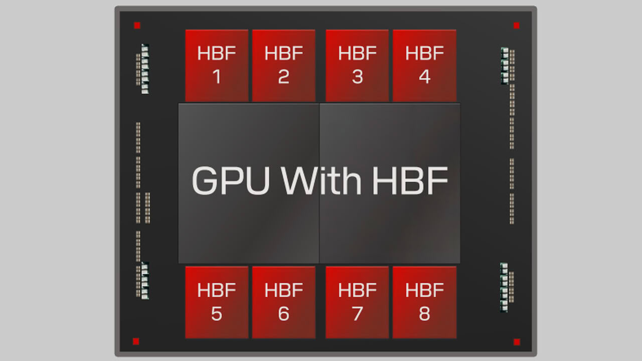
According to a DigiTimes report today, Micron is researching high-endurance NAND flash modules. The company plans to deploy them closer to the GPU, rather than connecting them through multiple protocols to a storage pool located farther away, as in traditional storage solutions.
According to the report, Micron is exploring how to move NAND flash even closer to the GPU, aiming to provide a compromise between storage density and endurance. The product is currently referred to as “near-GPU NAND” and can be used to handle workloads that do not require ultra-low latency or high bandwidth.
This approach would allow the GPU to directly access NAND storage pools with capacities of hundreds of GB. The storage could be placed directly inside the GPU package or on a PCB, operating similarly to solutions such as HBM and GDDR7. Compared with traditional TLC or QLC NAND, these NAND chips would offer lower storage density, with the focus on improving I/O speed and bandwidth.
This storage layer would sit between graphics memory and conventional storage, serving as a high-speed cache layer. It would therefore be particularly suitable for running larger AI large language models. Once deployed, the solution could prevent LLM inference from being constrained by graphics memory capacity.